Electronics and Optics Hardware Development Lifecycle
Opto-Electronic Intelligence
Design and Development for Opto-Electronic Hardware
- Requirements -> Test Specs -> Hardware Development
- Hardware Development
- Modularisation into testable entities
- Rapid design iteration for early prototypes
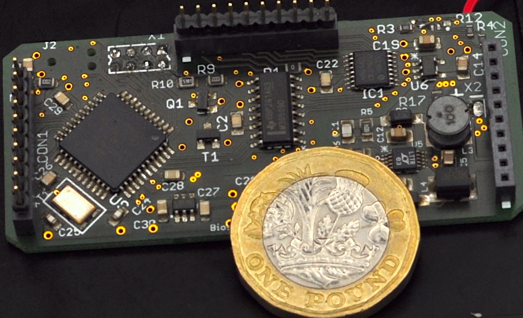
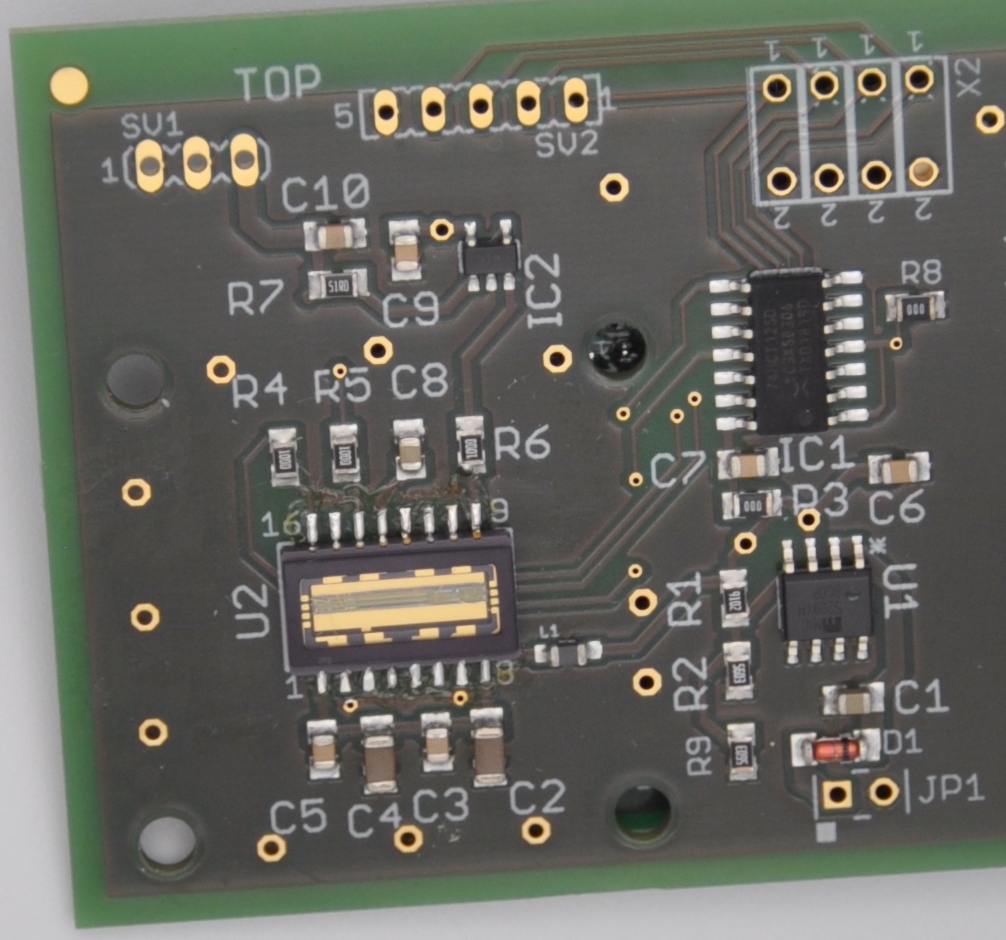
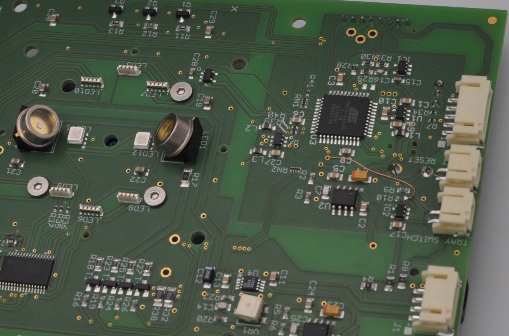
- Schematics, module PCBs
- Characterisation and testing
- Integration of modules to complete system
- Integrated PCB with annotated schematics
- Acceptance Testing
- Design optimisation and pre-production.
- Release PCB
- Test Driven Development for hardware
- Continuous Integration (CI) setup from start
- Everything hosted on a Git repository of your choice.
- CI on the development machine with test harnesses
- Integration testing with Python based automated testing
- Hardware-in-loop (HIL) implemented when needed
- Efficient hardware design in KiCAD1 or Eagle CAD (Autodesk)
- up to 4 layers electronics PCB
- Quick turn-around for urgent electronic prototypes by experienced hand assembly
- Suited for up to 50 surface mount and 20 through-hole components
- All boards manufactured in Europe
- Preferred suppliers:
Included Services
- Requirements and Testing Documents
- Delivery of reproducible testing environment
- Tech-transfer; no holding out on knowledge
- Bill-of-materials (BOM)
- CAD output for records
All components sourced from reputable suppliers only:
- Digikey, Farnell, RS Components or Mouser
- Hamamatsu for higher spec photonic components (photodiodes and arrays)
- Comar Optics, Edmund Optics, Thorlabs for Opto-Mechanical Components
PCBs Sourced from UK/Europe only Up to 3 PCBs can be hand-assembled for rapid-turnaround Small batch can be ordered by machine assembly with turn-around time of 3 weeks
Footnotes
KiCAD is a free and open-source EDA https://www.kicad.org/. It is used and supported by several companies and research institure including CERN https://ohwr.org/project/cern-kicad/wikis/home↩︎